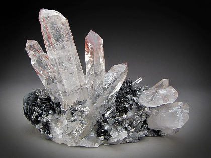
8. Gypsum (Calcium Sulfate Dihydrate)
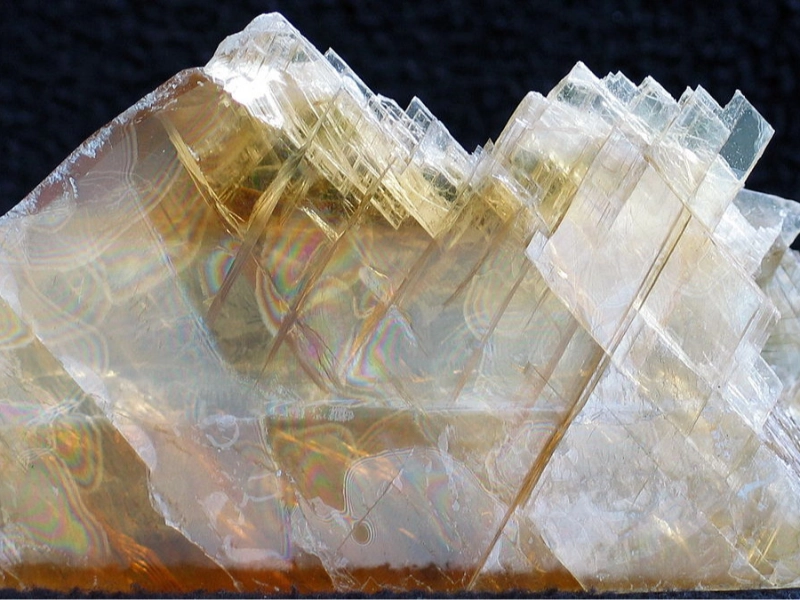
When considering electronics, one might not start with gypsum, a soft sulphate mineral with the chemical formula CaSO4·2H2O. Nevertheless, this adaptable material is very vital for the manufacturing of printed circuit boards (PCBs), the basis of almost all electronic equipment. The usage of gypsum in electronics manufacture shows how even apparently unrelated materials can become indispensable for the manufacturing of advanced components.
When producing PCBs, gypsum is mostly used as a masking agent during the etching process. Making PCBs requires designing complex patterns of electrical traces on a non-conductive substrate usually composed of fibreglass reinforced epoxy resin. Within the electronic gadget, these traces create the channels for electrical signals. These patterns must be created by precisely and under control etching, removing undesired copper from the board to leave just the intended circuit pattern.
Here’s where gypsum finds use. The places of the PCB that shouldn’t be etched are covered with a gypsum-based resist. Usually a combination of gypsum and other minerals, the resist can be applied precisely using screen printing or photolithography. Applied and dried, this gypsum-based resist shields the underlying copper from the etching chemicals.
Many of gypsum’s characteristics help to explain its success in this use. First, generally acidic solutions or alkaline ammonia-based compounds, gypsum is chemically inert to the etchants used in PCB manufacture. This inertness guarantees that the resist stays whole during the etching operation, therefore safeguarding the copper traces it covers. Second, once the etching process is over, gypsum can be readily removed usually by washing with water or a mild solvent. The next stages in PCB manufacture, such applying solder mask or surface treatments, depend on this simple removal.
Moreover, the capacity of gypsum to be finely ground and blended into stable suspensions enables the development of resist materials with outstanding resolution. Producing the progressively thin and densely packed circuit patterns needed by contemporary electronic gadgets depends on this high resolution. The capacity to produce ever-finer circuit patterns becomes increasingly important as electronics continue to shrink and becoming more complicated; the part gypsum plays in allowing this precision grows more important as well.
Additionally with environmental consequences is the usage of gypsum in PCB manufacture. Being a naturally occurring mineral, gypsum is very plentiful and easier to obtain than other manufactured substitutes with less effect on the surroundings. Furthermore, gypsum’s water solubility makes it possible to often treat PCB manufacturing process waste more readily than if more persistent chemicals were utilised.
Apart from its function in PCB production, gypsum has additional, though more indirect uses in the electronics sector. For example, specialised plasters and cements used in the building of clean rooms and other regulated conditions where electronic components are fabricated or assembled depend on gypsum. Gypsum-based products are fit for these delicate settings because of their low dust and particle emissions.
Gypsum is extracted and processed for use in electronics and other sectors through numerous stages. Usually, gypsum comes from either open-pit mining or subterranean deposits. To get the right particle size, the raw gypsum is next ground and screened. For high-purity uses like electronics, the gypsum may undergo further processing including washing to remove impurities and calcination to create anhydrous calcium sulphate, which can then be rehydrated under controlled conditions to generate gypsum of the necessary purity and consistency.
The use of materials like gypsum in manufacturing processes may change as the electronics sector develops with tendencies towards more compact devices, flexible electronics, and three-dimensional circuit structures. Investigating novel resist materials and etching methods might inspire changes in gypsum use or the creation of substitutes. Nonetheless, the basic characteristics of gypsum that make it beneficial in PCB manufacture—its chemical inertness, simplicity of application and removal, and capacity to produce high-resolution patterns—indicate that it will probably remain so in electronics manufacture for the foreseeable future.
In essence, even if gypsum might not be a component of the finished electronic goods we consume, its importance in the PCB manufacturing process renders it a necessary component in the electronics sector. The usage of gypsum in this high-tech application shows the interdependence of many sectors and materials as well as how conventional minerals still play fresh and vital roles in the manufacture of modern technologies.